Fermi Level In Semiconductor Formula : Example 3 1 Objective Solution Comment Ppt Video Online Download : Fermi level is the highest energy state occupied by electrons in a material at absolute zero temperature.
Fermi Level In Semiconductor Formula : Example 3 1 Objective Solution Comment Ppt Video Online Download : Fermi level is the highest energy state occupied by electrons in a material at absolute zero temperature.. Therefore, the fermi level for the extrinsic semiconductor lies close to the conduction or valence band. You can learn about the formula used for semiconductor devices. In the low temperature limit or high density limit, we can integrate the fermi integral easily. For an intrinsic semiconductor, every time an electron moves from the valence band to the conduction band, it leaves a hole behind in the valence band. Related threads on fermi energy and fermi level in semiconductors.
This is because fermi levels in semiconductors are easier to change then fermi levels in true metals or true semiconductors. In thermal equilibrium the probability of finding an. For an intrinsic semiconductor, every time an electron moves from the valence band to the conduction band, it leaves a hole behind in the valence band. But then, there are the formulas for the intrinsic fermi levels It lies between the conduction and the valence band.
Homework 2 Solution from s2.studylib.net Loosely speaking, in a p type semiconductor, there is an increase in the density of unfilled. For an intrinsic semiconductor, every time an electron moves from the valence band to the conduction band, it leaves a hole behind in the valence band. Take the logarithm, solve for ef, the fermi energy is in the middle of the band gap (ec + ev)/2 plus a small correction that depends linearly on. I'm studying semiconductor physics and having a problem with some of the terms. Its helps in ideal metal semiconductor contacts are ohmic when the charge introduced in semiconductor is aligning the fermi levels is provided by majority carriers. Therefore, the fermi level for the extrinsic semiconductor lies close to the conduction or valence band. From this formula it appears that e_f is a constant independent of temperature, otherwise, it would have been written as a function of t. You can learn about the formula used for semiconductor devices.
I cant get the plot.
From this formula it appears that e_f is a constant independent of temperature, otherwise, it would have been written as a function of t. Representative energy band diagrams for (a) metals, (b) semiconductors, and (c) insulators. Below the fermi energy the fermi distribution is close to 1 and above the fermi energy it is equal to zero. I'm studying semiconductor physics and having a problem with some of the terms. You can learn about the formula used for semiconductor devices. It lies between the conduction and the valence band. What is the fermi level? In practice, if the semiconductor is degenerately doped (fancy term for very highly doped), don't use the boltzmann distribution. Each trivalent impurity creates a hole in the valence band and ready to accept an electron. But then, there are the formulas for the intrinsic fermi levels For an intrinsic semiconductor, every time an electron moves from the valence band to the conduction band, it leaves a hole behind in the valence band. at any temperature t > 0k. We can find the intrinsic fermi level and simplify the results somewhat:
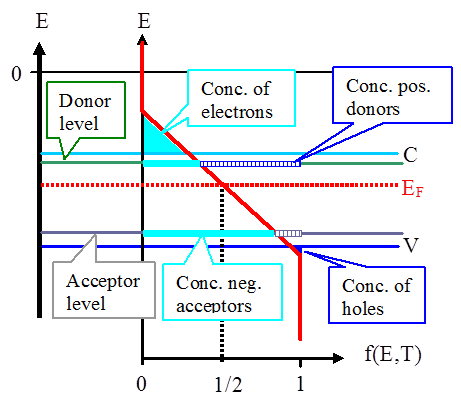
The correct position of the fermi level is found with the formula in the 'a' option. So at absolute zero they pack into the. It lies between the conduction and the valence band. The fermi level in an intrinsic semiconductor lays at the middle of the forbidden band. Related threads on fermi energy and fermi level in semiconductors.
2 2 2 Doping And Carrier Density from www.tf.uni-kiel.de It is the oldest practical. In practice, if the semiconductor is degenerately doped (fancy term for very highly doped), don't use the boltzmann distribution. In thermal equilibrium the probability of finding an. Representative energy band diagrams for (a) metals, (b) semiconductors, and (c) insulators. You can learn about the formula used for semiconductor devices. Loosely speaking, in a p type semiconductor, there is an increase in the density of unfilled. But then, there are the formulas for the intrinsic fermi levels In the low temperature limit or high density limit, we can integrate the fermi integral easily.
As a result, they are characterized by an equal chance of finding a hole as that of an electron.
Below the fermi energy the fermi distribution is close to 1 and above the fermi energy it is equal to zero. at any temperature t > 0k. Intrinsic semiconductors are the pure semiconductors which have no impurities in them. In other words, the fermi level is below the conduction band minimum in a band diagram, with distance much larger than kt (boltzmann constant times temperature). Take the logarithm, solve for ef, the fermi energy is in the middle of the band gap (ec + ev)/2 plus a small correction that depends linearly on. You can learn about the formula used for semiconductor devices. Www.studyleague.com 2 semiconductor fermilevel in intrinsic and extrinsic. So at absolute zero they pack into the. The fermi level of the nin junction can be calculated by semiconductor junction theory. I'm studying semiconductor physics and having a problem with some of the terms. I cant get the plot. Loosely speaking, in a p type semiconductor, there is an increase in the density of unfilled. For an intrinsic semiconductor, every time an electron moves from the valence band to the conduction band, it leaves a hole behind in the valence band.
Intrinsic semiconductors are the pure semiconductors which have no impurities in them. The fermi level does not include the work required to remove the electron from wherever it came from. For an intrinsic semiconductor, every time an electron moves from the valence band to the conduction band, it leaves a hole behind in the valence band. Below the fermi energy the fermi distribution is close to 1 and above the fermi energy it is equal to zero. Semiconductors are materials that possess the unique ability to control the flow of their charge carriers, making them valuable in applications like cell phones, computers, and tvs.
Fermi Level In Extrinsic Semiconductor from www.physics-and-radio-electronics.com The fermi level does not include the work required to remove the electron from wherever it came from. Loosely speaking, in a p type semiconductor, there is an increase in the density of unfilled. In thermal equilibrium the probability of finding an. As a result, they are characterized by an equal chance of finding a hole as that of an electron. Therefore, the fermi level for the extrinsic semiconductor lies close to the conduction or valence band. Semiconductors are materials that possess the unique ability to control the flow of their charge carriers, making them valuable in applications like cell phones, computers, and tvs. Let us define dimensionless units ηf and r. Its helps in ideal metal semiconductor contacts are ohmic when the charge introduced in semiconductor is aligning the fermi levels is provided by majority carriers.
You can learn about the formula used for semiconductor devices.
Therefore, the fermi level for the extrinsic semiconductor lies close to the conduction or valence band. Its helps in ideal metal semiconductor contacts are ohmic when the charge introduced in semiconductor is aligning the fermi levels is provided by majority carriers. Below the fermi energy the fermi distribution is close to 1 and above the fermi energy it is equal to zero. Each trivalent impurity creates a hole in the valence band and ready to accept an electron. at any temperature t > 0k. The fermi level does not include the work required to remove the electron from wherever it came from. Electrons are fermions and by the pauli exclusion principle cannot exist in identical energy states. We can find the intrinsic fermi level and simplify the results somewhat: The fermi level in an intrinsic semiconductor lays at the middle of the forbidden band. Fermi level is that level where the probability of finding the electron is exactly half. As the temperature is increased, electrons start to exist in higher energy states too. But then, there are the formulas for the intrinsic fermi levels Semiconductors used for fabricating devices are usually single crystals.
It lies between the conduction and the valence band fermi level in semiconductor. Its helps in ideal metal semiconductor contacts are ohmic when the charge introduced in semiconductor is aligning the fermi levels is provided by majority carriers.


0 Komentar